

PCB Fabrication
Materials
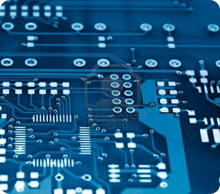
Conducting layers are typically made of thin copper foil. Insulating typically laminated together with epoxy resin. Well known prepreg materials used in the PCB industry are FR-2 (Phenolic cotton paper), FR-3 (Cotton paper and epoxy), FR-4 (Woven glass and epoxy), FR-5 (Woven glass and epoxy), FR-6 (Matte glass and polyester), G-10 (Woven glass and epoxy), CEM-1 (Cotton paper and epoxy), CEM-2 (Cotton paper and epoxy), CEM-3 (Woven glass and epoxy), CEM-4 (Woven glass and epoxy), CEM-5 (Woven glass and polyester). A PCB as a design on a computer and realized as a board assembly with populated components. The board is double sided, with through-hole plating, green solder resist, and white silkscreen printing. Both surface mount and through-hole components have been used.
Patterning (etching)
The vast majority of printed circuit boards are made by bonding a layer of copper over the entire substrate, sometimes on both sides, (creating a "blank PCB") then removing unwanted copper after applying a temporary mask (eg. by etching), leaving only the desired copper traces. A few PCBs are made by adding traces to the bare substrate (or a substrate with a very thin layer of copper) usually by a complex process of multiple electroplating steps. There are three common "subtractive" methods (methods that remove copper) used for the production of printed circuit boards:
- Silk screen printing uses etch-resistant inks to protect the copper foil. Subsequent etching removes the unwanted copper. Alternatively, the ink may be conductive, printed on a blank (non-conductive) board. The latter technique is also used in the manufacture of hybrid circuits.
- Photoengraving uses a photomask and chemical etching to remove the copper foil from the substrate. The photomask is usually prepared with a photoplotter from data produced by a technician using CAM, or computer-aided manufacturing software. Laser-printed transparencies are typically employed for phototools; however, direct laser imaging techniques are being employed to replace phototools for high-resolution requirements.
- PCB milling uses a two or three-axis mechanical milling system to mill away the copper foil from the substrate. A PCB milling machine (referred to as a 'PCB Prototyper') operates in a similar way to a plotter, receiving commands from the host software that control the position of the milling head in the x, y, and (if relevant) z axis. Data to drive the Prototyper is extracted from files generated in PCB design software and stored in HPGL or Gerber file format. "Additive" processes also exist. The most common is the "semi-additive" process. In this version, the unpatterned board has a thin layer of copper already on it. A reverse mask is then applied. (Unlike a subtractive process mask, this mask exposes those parts of the substrate that will eventually become the traces.) Additional copper is then plated onto the board in the unmasked areas; copper may be plated to any desired weight. Tin-lead or other surface platings are then applied. The mask is stripped away and a brief etching step removes the now-exposed original copper laminate from the board, isolating the individual traces. The additive process is commonly used for multi-layer boards as it facilitates the plating-through of the holes (to produce conductive vias) in the circuit board.
Lamination
Some PCBs have trace layers inside the PCB and are called multi-layer PCBs. These are formed by bonding together separately etched thin boards.
Drilling
Holes, or vias, through a PCB are typically drilled with tiny drill bits made of solid tungsten carbide. The drilling is performed by automated drilling machines with placement controlled by a drill tape or drill file. These computer-generated files are also called numerically controlled drill (NCD) files or "Excellon files". The drill file describes the location and size of each drilled hole. When very small vias are required, drilling with mechanical bits is costly because of high rates of wear and breakage. In this case, the vias may be evaporated by lasers. Laser-drilled vias typically have an inferior surface finish inside the hole. These holes are called micro vias. It is also possible with controlled-depth drilling, laser drilling, or by pre-drilling the individual sheets of the PCB before lamination, to produce holes that connect only some of the copper layers, rather than passing through the entire board. These holes are called blind vias when they connect an internal copper layer to an outer layer, or buried vias when they connect two or more internal copper layers and no outer layers. The walls of the holes, for boards with 2 or more layers, are plated with copper to form plated-through holes that electrically connect the conducting layers of the PCB. For multilayer boards, those with 4 layers or more, drilling typically produces a smear comprised of the bonding agent in the laminate system. Before the holes can be plated through, this smear must be removed by a chemical de-smear process, or by plasma-etch.
Exposed Conductor Plating and Coating
The places to which components will be mounted are typically plated, because bare copper oxidizes quickly, and therefore is not readily solderable. Traditionally, any exposed copper was plated with solder by hot air solder levelling (HASL). This solder was a tin-lead alloy, however new solder compounds are now used to achieve compliance with the RoHS directive in the EU, which restricts the use of lead. Other platings used are OSP (organic surface protectant), immersion silver (IAg), immersion tin, electroless nickel with immersion gold coating (ENIG), and direct gold. Edge connectors, placed along one edge of some boards, are often gold plate. Electrochemical migration (ECM) is the growth of conductive metal filaments on or in a printed circuit board (PCB) under the influence of a DC voltage bias.
Solder Resist
Areas that should not be soldered to may be covered with a polymer solder resist (solder mask) coating. The solder resist prevents solder from bridging between conductors and thereby creating short circuits. Solder resist also provides some protection from the environment.
Screen Printing
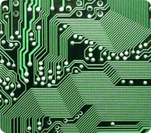
Line art and text may be printed onto the outer surfaces of a PCB by screen printing. When space permits, the screen print text can indicate component designators, switch setting requirements, test points, and other features helpful in assembling, testing, and servicing the circuit board. Screen print is also known as the silk screen, or, in one sided PCBs, the red print. Lately some digital printing solutions have been developed to substitute the traditional screen printing process. This technology allows printing variable data onto the PCB, including serialization and barcode information for traceability purposes.
Test
Unpopulated boards may be subjected to a bare-board test where each circuit connection (as defined in a netlist) is verified as correct on the finished board. For high-volume production, a Bed of nails tester, a fixture or a Rigid needle adapter is used to make contact with copper lands or holes on one or both sides of the board to facilitate testing. A computer will instruct the electrical test unit to send a small amount of current through each contact point on the bed-of-nails as required, and verify that such current can be seen on the other appropriate contact points. A "short" on a board would be a solid connection where there should be no connection. An "open" is between two points that should be connected and are not. For small- or medium-volume boards, flying-probe and flying-grid testers use moving test heads to make contact with the copper/silver/gold/solder lands or holes to verify the electrical connectivity of the board under test.
At Integrated Circuit Technologies we are here for our customers. We have assembled "General Information" as a resource for our customers on how Printed Circuit Boards are manufactured. For detailed information on your specific project please give us a call.
Contact Us

